캐리어 테이프 원자재
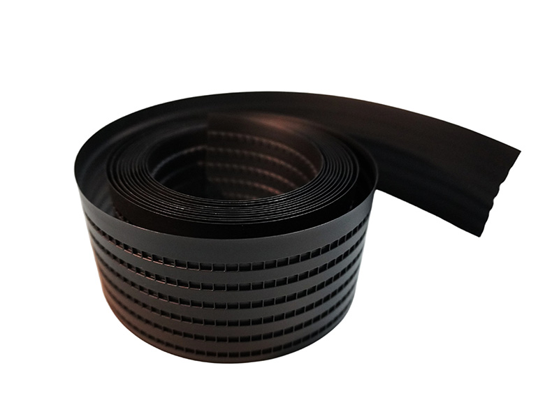
High-Performance Thermoplastic Sheets for Precision Carrier Tape Forming
Introduction
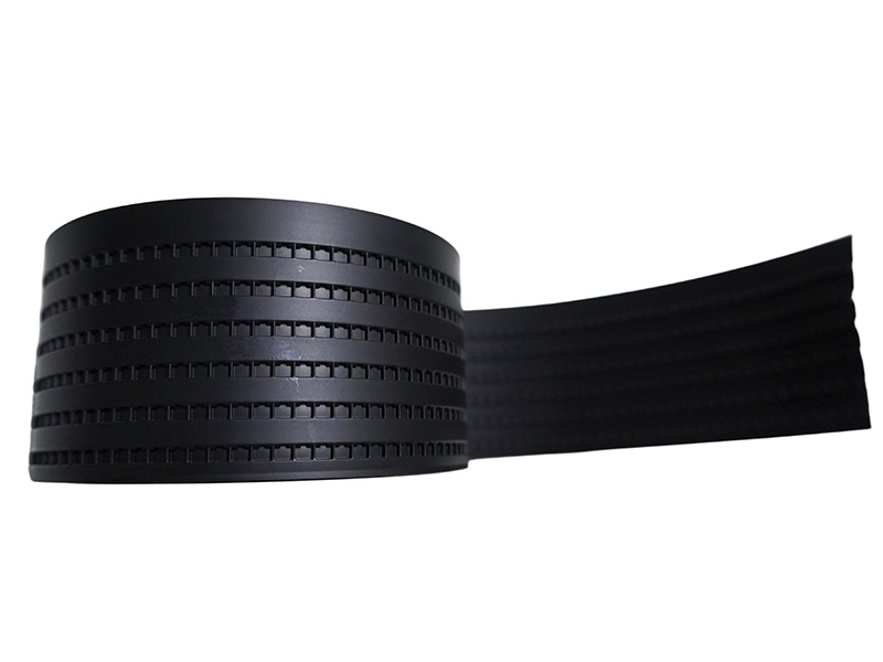
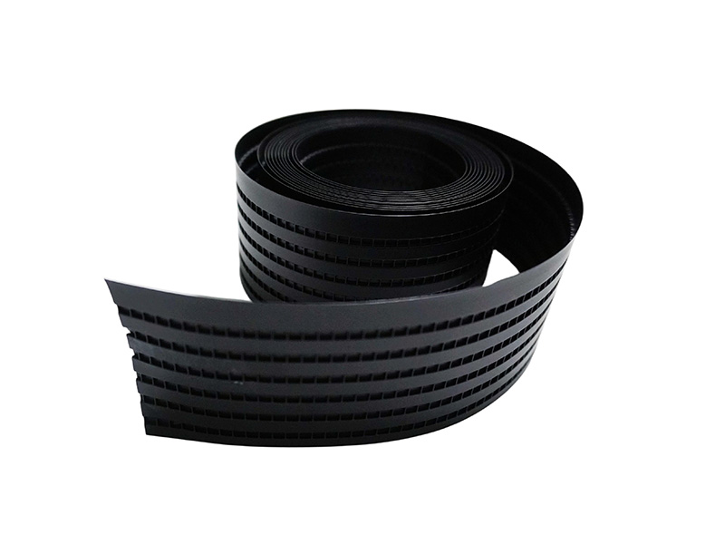
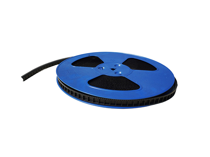
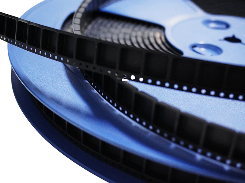
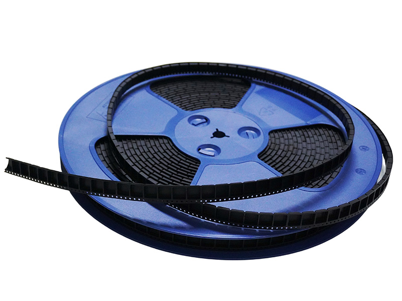
Carrier tape is the backbone of modern surface-mount technology (SMT) packaging—a precision-engineered thermoplastic strip that holds electronic components during storage, shipping, and automated assembly. The quality of the finished carrier tape begins with the raw material. As the industry standard EIA-481 and IEC 60286-3 specify, carrier tapes must meet stringent dimensional and electrostatic requirements to ensure compatibility with automated placement equipment .
The selection of raw materials directly determines pocket-forming quality, dimensional stability, electrostatic discharge (ESD) performance, and overall production efficiency. Whether manufacturing semiconductor IC tapes, LED packaging strips, or consumer electronics component carriers, the material choice impacts every downstream process—from forming station throughput to SMT placement yield.
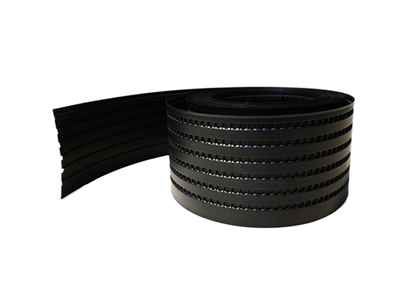
Thermoplastic sheets for carrier tape production are typically supplied in roll form, with thicknesses ranging from 0.2mm to 0.5mm and widths up to 700mm. These materials undergo a multi-stage processing journey: preheating to remove moisture, forming at controlled temperatures, precision punching, slitting, and final rewinding.
Common Carrier Tape Materials: PC, PS, and PET
The most widely used materials for embossed carrier tape production are Polycarbonate (PC) , Polystyrene (PS) , and Polyethylene Terephthalate (PET) . Each offers distinct properties that make it suitable for specific applications.
Polycarbonate (PC)
Polycarbonate is a transparent, amorphous thermoplastic known for its exceptional impact strength and dimensional stability . It is the preferred material for demanding applications where pocket integrity and optical clarity are critical.
| Property | Characteristic |
|---|---|
| Transparency | High optical clarity for automated inspection |
| Heat Resistance | Up to 120–130°C |
| Impact Strength | Excellent; suitable for deep cavities (>10mm) |
| Surface Resistivity | Customizable (conductive grades available) |
| Typical Applications | Connectors, relays, shielding covers, large inductors |
Industry sources confirm that PC is particularly suitable for deep-cavity carrier tapes and applications where mechanical strength is paramount . Its resistance to impact makes it ideal for heavy or sensitive components that require robust protection during shipping.
Polystyrene (PS)
Polystyrene is a cost-effective, general-purpose thermoplastic widely used in carrier tape production. It offers excellent formability and surface finish at a lower cost point than PC.
| Property | Characteristic |
|---|---|
| Transparency | Good clarity |
| Heat Resistance | Up to 80–90°C |
| Formability | Excellent for shallow cavities (<8mm) |
| Surface Resistivity | Customizable (conductive grades available) |
| Typical Applications | Chip resistors, capacitors, SOT-23, SOP packages, LEDs |
PS is the material of choice for high-volume, cost-sensitive production and is commonly available in both conductive and non-conductive grades . Industry literature notes that PS carrier tapes are widely used for passive components and standard IC packages where the pocket depth requirements are moderate .
Conductive PS: Carbon black is added during compounding to achieve surface resistivity in the range of 10⁵–10¹¹ Ω/sq . This is critical for ESD-sensitive components such as MOSFETs and ICs. As documented in manufacturing patents, conductive PS formulations typically contain 10–30% conductive carbon black by mass .
PET and APET
PET (Polyethylene Terephthalate) and its amorphous variant APET are increasingly popular due to their excellent optical clarity, low forming shrinkage, and balanced cost-performance ratio.
| Property | Characteristic |
|---|---|
| Transparency | Comparable to PC |
| Heat Resistance | 85–100°C |
| Shrinkage | Low; good dimensional stability |
| Surface Resistivity | Permanent antistatic capability (10⁶–10⁸ Ω/sq) |
| Typical Applications | Automotive electronics, power modules, halogen-free applications |
Industry sources indicate that APET offers low forming shrinkage, making it particularly suitable for thin components (thickness <2mm) where dimensional precision is critical . Its transparency is comparable to PC, enabling reliable optical inspection during production.
Material Specifications and Selection Criteria
Thickness and Width
Carrier tape raw materials are supplied in sheet form with precise thickness control:
- Typical thickness range: 0.2mm – 0.5mm
- Typical roll width: Up to 700mm
- Final tape widths (after slitting): 8mm, 12mm, 16mm, 24mm, 32mm, 44mm, 56mm, 72mm, 88mm, 104mm
Thickness selection is critical: materials that are too thin may not form deep pockets (K0 > 10mm) without tearing, while materials that are too thick may not form shallow pockets cleanly.
Electrostatic Discharge (ESD) Properties
ESD protection is a primary consideration in carrier tape design. The surface resistivity range required depends on component sensitivity:
| Resistivity Range | Classification | Application |
|---|---|---|
| 10⁵–10⁹ Ω/sq | Conductive | Highly ESD-sensitive components (ICs, MOSFETs) |
| 10⁹–10¹¹ Ω/sq | Antistatic | Standard components |
| >10¹¹ Ω/sq | Non-conductive | Components not ESD-sensitive |
Conductive additives—typically carbon black, carbon nanotubes, or ionic antistatic agents—are compounded into the base polymer to achieve the required resistivity .
Mechanical Properties
Key mechanical properties that determine processing and performance:
- Yield strength — Determines the material’s resistance to stretching during forming. For PC: ~50 MPa; for PS: ~25–45 MPa .
- Tensile modulus — Affects how the material behaves under tension during forming and slitting. PC: ~1900 MPa; PS: ~1500–1800 MPa .
- Impact resistance — Critical for components requiring protection during shipping.
- Camber (flatness) — Industry standard requires ≤1mm over 250mm length .
Material Selection by Application
| Application | Recommended Material | Key Considerations |
|---|---|---|
| Semiconductor ICs | Conductive PC | Heat resistance, impact strength, deep cavity capability |
| Passive Components | Conductive PS | Cost-effectiveness, high-volume production |
| LED Packages | PS (shallow) / PC (deep) | Surface quality, transparency for inspection |
| Automotive Electronics | APET / PET | Low shrinkage, thermal stability |
| Large Connectors | PC | Deep cavity capability, mechanical strength |
| Power Modules | APET | Shrinkage control, dimensional precision |
Material Handling and Storage
Raw materials for carrier tape production require proper handling and storage to maintain quality:
- Moisture control: Thermoplastics are hygroscopic and must be dried before processing to prevent bubbles and forming defects
- Temperature: Store in a cool, dry environment (typically 15–25°C)
- ESD precautions: Conductive materials should be stored in static-controlled environments
- Shelf life: Most thermoplastic sheets have a recommended shelf life of 12–24 months from manufacture
Quality Standards and Compliance
Carrier tape raw materials and finished products are governed by international standards:
| Standard | Scope |
|---|---|
| EIA-481-D | Embossed carrier tape specifications for SMT components |
| IEC 60286-3 | Dimensions and requirements for carrier tape packaging |
| IEC 61249-2-51 | Base materials for IC carrier tape |
| RoHS/REACH | Environmental compliance for hazardous substances |
| IPC/JEDEC J-STD-033 | Moisture sensitivity handling requirements |
Why Material Choice Matters
The raw material you select determines:
- Forming yield — Materials with inconsistent thickness or improper moisture content cause rejects
- Production speed — PC and PS require different forming temperatures and speeds
- Dimensional stability — Shrinkage during cooling affects critical dimensions (E, F, P0, P1)
- ESD performance — Inadequate resistivity leads to component damage
- Customer acceptance — Non-compliant materials result in rejection
Industry data shows that carriers with consistent pocket geometry and ESD compliance achieve significantly higher SMT placement yield rates .
Conclusion
Carrier tape raw materials—PC, PS, and PET—are the foundation of precision electronic component packaging. Selecting the right material based on application requirements, processing conditions, and ESD needs is essential for achieving consistent quality and maximizing production efficiency.
For detailed specifications, material samples, or technical consultation, contact our team. We are happy to assist in selecting the optimal material for your carrier tape production needs.
 한국어
한국어  English (UK)
  Bahasa Indonesia
  Tiếng Việt
  Русский